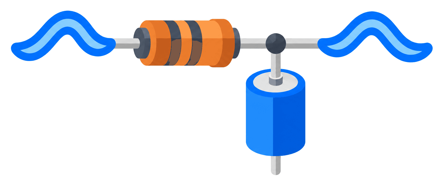
Astable circuit
Repeating oscillator using RA, RB and the timing capacitor.
Timing circuit tool
Calculate standard 555 monostable pulse width or astable frequency, high time, low time and duty cycle. Design mode suggests practical E-series timing components for a target.
Frequency
3.6075 Hz
Period
277.2 ms
Duty cycle
62.5%
High time
173.25 ms
Low time
103.95 ms
Practical range
The timing result sits inside the 0.1 Hz to 5 MHz quick-reference range.
Connect each formula term to the real pin and component path. These drawings are functional references, not complete production schematics.
Repeating oscillator using RA, RB and the timing capacitor.
Triggered one-shot using one timing resistor and capacitor.
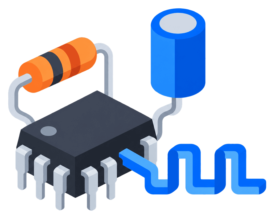
DIP-8 pin roles used by both reference circuits.
Select the operating mode first because monostable and astable circuits use different equations and component arrangements.
Monostable mode produces one pulse per trigger. Astable mode continuously alternates between high and low states.
Evaluate calculates from entered values. Design searches practical E12 or E24 values for a target pulse width or frequency.
Check the proposed resistance, capacitance, duty cycle and frequency against the exact timer variant, supply and load in its datasheet.
The calculator uses the conventional first-order equations for the common monostable and two-resistor astable connections.
Monostable pulse
t = 1.1 × R × C
Astable frequency
f = 1.44 / ((RA + 2RB) × C)
Astable high time
tH = 0.693 × (RA + RB) × C
Astable low time
tL = 0.693 × RB × C
Astable duty cycle
D = (RA + RB) / (RA + 2RB)
In the standard astable connection, the capacitor charges through RA and RB but discharges through RB. That topology keeps the ideal duty cycle above 50% unless the charge and discharge paths are modified.
The equations are nominal. Threshold accuracy, leakage, capacitor tolerance, timing resistance limits, output loading and device technology affect the result. Use the datasheet for the exact NE555, CMOS 555 or compatible part and validate critical timing on hardware.
A close calculated target is only the start of a robust timer design.
Very low resistance can overload the discharge transistor; very high resistance makes leakage and input currents more significant. Follow the selected device datasheet.
Large electrolytic capacitors can have wide tolerance and leakage. Choose a capacitor technology suited to the time range and required repeatability.
Place local bypass capacitance close to the timer and keep high-current output paths away from the threshold and trigger nodes.
The conventional two-resistor astable circuit cannot produce a nominal duty cycle below 50%. Use a modified charge/discharge path when that is required.
Monostable mode waits for a trigger and produces one timed pulse. Astable mode free-runs and produces a repeating waveform.
The timing capacitor charges through RA plus RB but discharges only through RB, so the calculated high interval is always longer than the low interval.
Component tolerance, capacitor leakage, timer thresholds, supply conditions, wiring parasitics and loading all contribute error.
They are useful nominal equations for the standard topology, but operating limits and errors differ by device. Check the exact CMOS timer datasheet before choosing components.
Explore the underlying RC exponential response and settling intervals.
Open resourceCheck how the same R and C values behave in a first-order filter.
Open resourceBrowse the current set of tested electrical and RF calculators.
Open resourceTechnical references: Texas Instruments: NE555 product page, Texas Instruments: NA555, NE555 and SA555 datasheet